With the launch of the new iPad Pro models at WWDC this year, Apple introduced new 10.5-inch and 12.9-inch devices that both came with an A10X Fusion Chip, which is said to deliver 30 percent faster CPU performance than previous-generation iPad Pro models and 40 percent faster graphics performance. The manufacturing process by which Apple fabricated the chip was never clear, but now TechInsights has confirmed that the A10X chip was built using a 10-nanometer FinFET process.
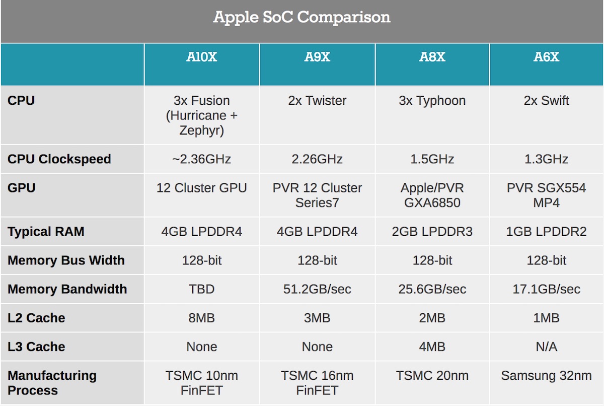
Specifically, the the chips were built using Taiwan Semiconductor Manufacturing Company’s new 10-nanometer FinFET process, making the A10X the first TSMC 10-nanometer chip to show up in a consumer device. In comparison, the A9 and A10 were built using a 16-nanometer process, the A8 used a 20-nanometer process, and the A7 used a 28-nanometer process. As AnandTech pointed out, the A9, A8, and A7 were all iPhone chips that debuted a new process node at the time of their manufacturing, so it’s unclear why Apple decided to fabricate a mid-generation X-series chip within an iPad on a new process node this time around.

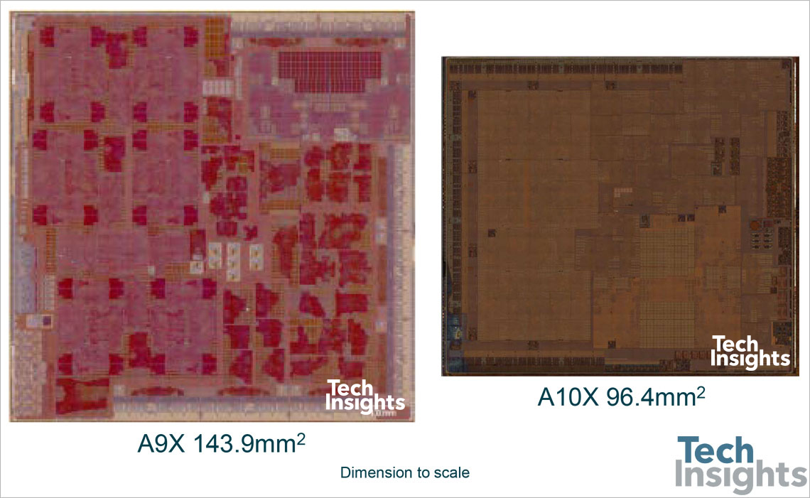
Compared to previous SoC standards not in the X-series, the A10X (96.4mm squared) is 24 percent smaller than the A10 (125mm squared), and 9 percent smaller than the A9 (104.5mm squared). For previous X-series chips, the A10X is 34 percent smaller than the A9X and 20 percent smaller than the A6X. “In other words, Apple has never made an iPad SoC this small before,” AnandTech explained.
Ultimately what this means is that in terms of design and features, A10X is relatively straightforward. It’s a proper pipecleaner product for a new process, and one that is geared to take full advantage of the die space savings as opposed to spending those savings on new features/transistors.
TechInsights‘ die shot revealed some details about the floorplan of the A10X, including 12 GPU clusters on the left and CPU cores on the right, but otherwise the shots weren’t clean enough to draw any more information about the chip that Apple hasn’t already confirmed. The “conservative” SoC is said to be largely similar to the A9X SoC, with a few differences: the A10X includes 3 Fusion CPU core pairs, up from 2 on the A10 and A9X, and has seen a bump in the L2 cache to 8MB, up from 3MB on the A9X.

The GPU sticks with 12 clusters, seen in the floorplan, which the A9X also had, meaning that “the only major change is the CPU cores.” So the A10X is more powerful than the A9X at a significant decrease in die size, as is typical with Apple’s manufacturing processes. One confirmation offered by the die shot appears to be that Apple is still using Imagination Technology’s PowerVR architecture in the A10X SoC. This past April, Apple told the manufacturer it would stop using its graphics technology in its devices within two years time, because the Cupertino company is developing its own independent graphics processing chips.
In March it was reported that TSMC was gearing up to begin production on the iPhone 8’s A11 chip, and after a delay that production has officially begun, also using the manufacturer’s 10-nanometer FinFET process. In general, the jump to 10-nanometer instead of 16-nanometer will yield chips that are more power efficient, resulting in user experiences that are snappier.
For TSMC, the 10-nanometer FinFET process is predicted to be a short-lived node, as it’s said that the manufacturer is gearing up to jump to a 7-nanometer process in 2018. Other manufacturers, including Samsung and Intel, are believed to stick with 10-nanometer as their main fabrication process for a bit longer than TSMC.


