Bipolar Junction Transistor (BJT): DC and AC Analysis
The invention of the transistor was the beginning of a technological revolution that is still continuing. All of the complex electronic devices and systems today are an outgrowth of early developments in semiconductor transistors. Two basic types of transistors are the bipolar junction transistor (BJT), and the field-effect transistor (FET), which we will cover later.
The BJT is used in two broad areas—as a linear amplifier to boost or amplify an electrical signal and as an electronic switch.
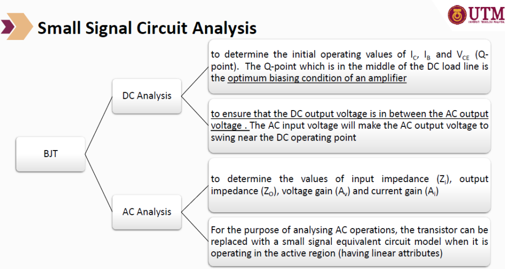
Type of BJT Analysis
Bipolar Junction Transistor (BJT) Structure
The BJT is constructed with three doped semiconductor regions separated by two pn junctions, as shown in the epitaxial planar structure in Figure 1(a). The three regions are called emitter, base, and collector. Physical representations of the two types of BJTs are shown in Figure 1(b) and 1(c). One type consists of two n regions separated by a p region (npn), and the other type consists of two p regions separated by an n region (pnp). The term bipolar refers to the use of both holes and electrons as current carriers in the transistor structure.
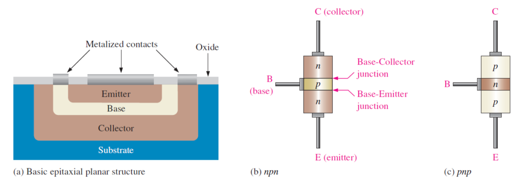
The pn junction joining the base region and the emitter region is called the base-emitter junction. The pn junction joining the base region and the collector region is called the base-collector junction, as indicated in Figure 2(b). A lead connects to each of the three regions, as shown. These leads are labeled E, B, and C for emitter, base, and collector, respectively. The base region is lightly doped and very thin compared to the heavily doped emitter and the moderately doped collector regions. Because of this difference in doping levels, the emitter and collector are not interchangeable. (The reason for this is discussed in the next section.) Figure 2 shows the schematic symbols for the npn and pnp bipolar junction transistors.
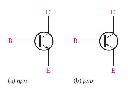
transistor) symbols [1]
BJT Basic Operation Region
Hereby, I share the lecture notes on BJT Basic Operation Region for you to understand before I further discuss the example and circuit analysis of BJT.
BJT Biasing Circuit: Common Emitter Configuration
Bear in mind, the current will flow in a conductor as long as voltage, the electrical pressure, is applied to the conductor. For the case of BJT CE configuration circuit as shown in figure below, the current will flow from positive terminal of VCC to the ground in two different paths according to the Kirchhoff’s Current Law (KCL) namely IB; the current that flow through the base of the BJT and IC; the current that flow through the collector of the BJT
Notes: To solve the circuit analysis of BJT, the capacitors need to be relocated and replaced with an open circuit.
Example 1
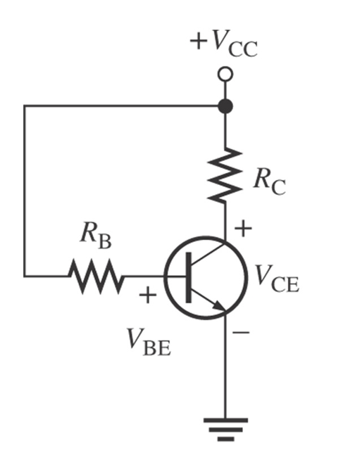
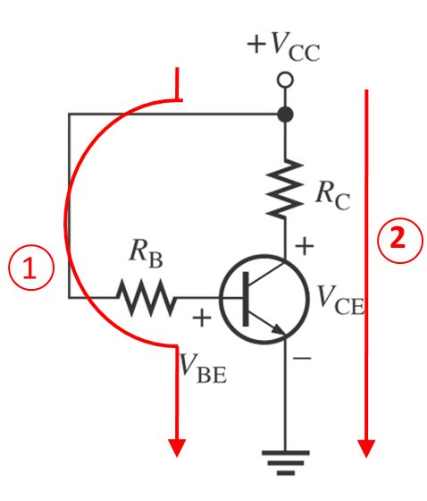
Here, you can locate two (2) main loops which are the base to emitter (BE) loop and collector to emitter loop (CE) by using the Kirchhoff’s Voltage Law (known as KVL).
From BE loop (1), we can deduce an equation as follows:
(A) VCC – IBRB – VBE = 0 —> Rearrange the equation to calculate IB
Meanwhile, from CE loop (2) using the KVL the equation will be like this:
VCC – ICRC – VCE = 0 —> Rearrange the equation to calculate VCE
(B) IC = BIB
Substituting (A) with (B) to get (C):
Now, lets try on this example!
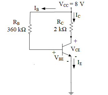
Find IBQ, ICQ, VCEQ, VCQ, VEQ and VBQ
Solution:

EXERCISE 1
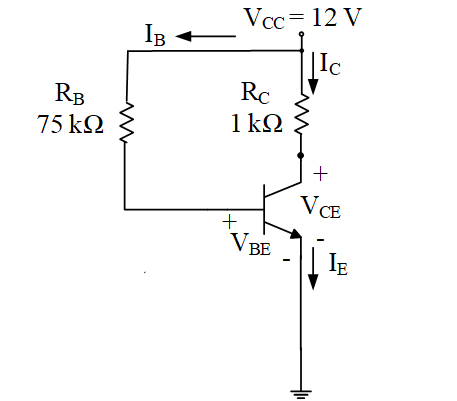
Find IBQ, ICQ, VCEQ, VCQ, VEQ and VBQ
Do send to me your answer through my email at nurnajahatulhuda@utm.my You can earn KFC voucher as a reward if you get all correct answer. All the best!
BJT AC analysis
Now, lets move on the other type of BJT analysis which is AC analysis. Hereby, I share the lecture notes on BJT AC analysis for you to revise.
After doing some revision on the attached material, you are required to solve the tutorials below in group. Concurrently, I ask my students to produce a video presentation to show the calculation and solution BRIEFLY.
Some of my students asked me…
” Why we need to work in group?”
“I think I can do it alone”
Study groups encourage members to think creatively and build strong communication skills which also help in refining understanding of the material. It has been proven that those who participate in study groups feel more confident and comfortable about reaching their academic goals.
From time to time, I will update the solutions solved by my students. Stay tuned!
Solutions Question 1, 2 and 11
Correction on the answer, the first one is not the saturation region. It is cut off region. This is because for silicon, the value is 0.7V. Since the VBE is not reach 0.7 V which is only 0.3 V, therefore it is considered reverse bias, NOT forward bias. Hence, the answer is cut off region. Make sure you know the operating region of BJT.
But, if the type of BJT is Germanium, it is saturation region.
Solutions Question 3, 4 and 5
Solutions Question 6, 7 and 8
Solutions Question 9 and 10
Now, what you have learnt from this topic?
Let’s click on the to test your knowledge through Quiz!
https://quizizz.com/admin/quiz/62e9fccfc34a4d001d147e44/bipolar-junction-transistor-bjt